Report an Error
NVIDIA GeForce RTX 5070 Ti
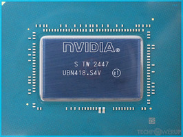
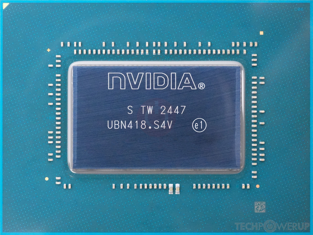
- Graphics Processor
- GB203
- Cores
- 8960
- TMUs
- 280
- ROPs
- 128
- Memory Size
- 16 GB
- Memory Type
- GDDR7
- Bus Width
- 256 bit
GPU
This product is not released yet.
Data on this page may change in the future.
Recommended Gaming Resolutions:
- 1920x1080
- 2560x1440
- 3840x2160
The GeForce RTX 5070 Ti will be an enthusiast-class graphics card by NVIDIA, that is expected to launch on February 20th, 2025. Built on the 5 nm process, and based on the GB203 graphics processor, in its GB203-200-A1 variant, the card supports DirectX 12 Ultimate. This ensures that all modern games will run on GeForce RTX 5070 Ti. Additionally, the DirectX 12 Ultimate capability guarantees support for hardware-raytracing, variable-rate shading and more, in upcoming video games. The GB203 graphics processor is a large chip with a die area of 378 mm² and 45,600 million transistors. Unlike the fully unlocked GeForce RTX 5080, which uses the same GPU but has all 10752 shaders enabled, NVIDIA has disabled some shading units on the GeForce RTX 5070 Ti to reach the product's target shader count. It features 8960 shading units, 280 texture mapping units, and 128 ROPs. Also included are 280 tensor cores which help improve the speed of machine learning applications. The card also has 70 raytracing acceleration cores. NVIDIA has paired 16 GB GDDR7 memory with the GeForce RTX 5070 Ti, which are connected using a 256-bit memory interface. The GPU is operating at a frequency of 2300 MHz, which can be boosted up to 2452 MHz, memory is running at 1750 MHz (28 Gbps effective).
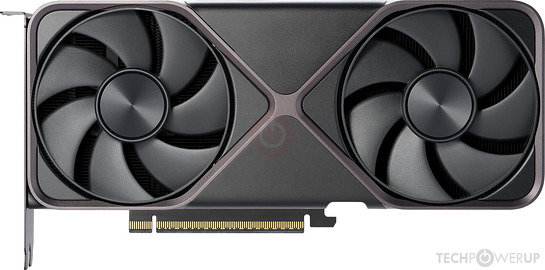
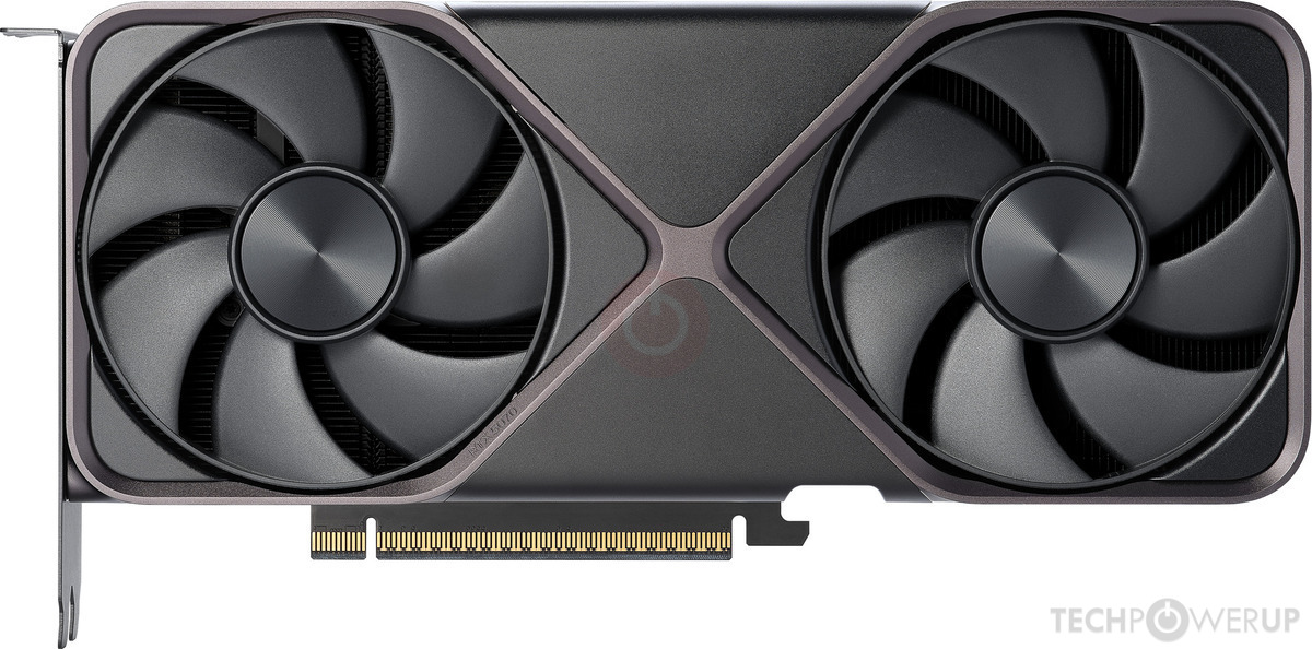
Being a dual-slot card, the NVIDIA GeForce RTX 5070 Ti draws power from 1x 16-pin power connector, with power draw rated at 300 W maximum. Display outputs include: 1x HDMI 2.1b, 3x DisplayPort 2.1b. GeForce RTX 5070 Ti is connected to the rest of the system using a PCI-Express 5.0 x16 interface. The card's dimensions are 304 mm x 137 mm x 48 mm, and it features a dual-slot cooling solution. Its price at launch will be 749 US Dollars.
Being a dual-slot card, the NVIDIA GeForce RTX 5070 Ti draws power from 1x 16-pin power connector, with power draw rated at 300 W maximum. Display outputs include: 1x HDMI 2.1b, 3x DisplayPort 2.1b. GeForce RTX 5070 Ti is connected to the rest of the system using a PCI-Express 5.0 x16 interface. The card's dimensions are 304 mm x 137 mm x 48 mm, and it features a dual-slot cooling solution. Its price at launch will be 749 US Dollars.
Graphics Processor
- GPU Name
- GB203
- GPU Variant
- GB203-200-A1
- Architecture
- Blackwell 2.0
- Foundry
- TSMC
- Process Size
- 5 nm
- Transistors
- 45,600 million
- Density
- 120.6M / mm²
- Die Size
- 378 mm²
Graphics Card
- Release Date
- Feb 20th, 2025
- Announced
- Jan 6th, 2025
- Generation
- GeForce 50
- Predecessor
- GeForce 40
- Production
- Unreleased
- Launch Price
- 749 USD
- Bus Interface
- PCIe 5.0 x16
Relative Performance
Based on TPU review data: "Performance Summary" at 1920x1080, 4K for 2080 Ti and faster.
Performance estimated based on architecture, shader count and clocks.
Clock Speeds
- Base Clock
- 2300 MHz
- Boost Clock
- 2452 MHz
- Memory Clock
-
1750 MHz
28 Gbps effective
Memory
- Memory Size
- 16 GB
- Memory Type
- GDDR7
- Memory Bus
- 256 bit
- Bandwidth
- 896.0 GB/s
Render Config
- Shading Units
- 8960
- TMUs
- 280
- ROPs
- 128
- SM Count
- 70
- Tensor Cores
- 280
- RT Cores
- 70
- L1 Cache
- 128 KB (per SM)
- L2 Cache
- 64 MB
Theoretical Performance
- Pixel Rate
- 313.9 GPixel/s
- Texture Rate
- 686.6 GTexel/s
- FP16 (half)
- 43.94 TFLOPS (1:1)
- FP32 (float)
- 43.94 TFLOPS
- FP64 (double)
- 686.6 GFLOPS (1:64)
Board Design
- Slot Width
- Dual-slot
- Length
- 304 mm
12 inches
- Width
- 137 mm
5.4 inches
- Height
- 48 mm
1.9 inches
- TDP
- 300 W
- Suggested PSU
- 700 W
- Outputs
- 1x HDMI 2.1b
3x DisplayPort 2.1b
- Power Connectors
- 1x 16-pin
- Board Number
- PG147 SKU 60
Graphics Features
- DirectX
- 12 Ultimate (12_2)
- OpenGL
- 4.6
- OpenCL
- 3.0
- Vulkan
- 1.4
- CUDA
- 10.1
- Shader Model
- 6.8
GB203 GPU Notes
| Ray Tracing Cores: 4th Gen Tensor Cores: 5th Gen NVENC: 9th Gen NVDEC: 6th Gen PureVideo HD: VP13 VDPAU: Feature Set M Latest Drivers: Windows 10 / 11: GeForce Release: Latest Quadro Release: Latest Data Center Release: Latest |
Retail boards based on this design (47)
| Name | GPU Clock | Boost Clock | Memory Clock | Other Changes |
|---|---|---|---|---|
| 2300 MHz | 2452 MHz | 1750 MHz | 306 mm/12 inches, Triple-slot | |
| 2300 MHz | 2452 MHz | 1750 MHz | 306 mm/12 inches, Triple-slot | |
| 2300 MHz | 2452 MHz | 1750 MHz | 329 mm/13 inches, Triple-slot | |
| 2300 MHz | 2452 MHz | 1750 MHz | 329 mm/13 inches, Triple-slot | |
| 2300 MHz | 2452 MHz | 1750 MHz | 332 mm/13.1 inches, Triple-slot | |
| 2300 MHz | 2452 MHz | 1750 MHz | 332 mm/13.1 inches, Triple-slot | |
| 2300 MHz | 2452 MHz | 1750 MHz | 316 mm/12.4 inches, Triple-slot | |
| 2300 MHz | 2452 MHz | 1750 MHz | 332 mm/13.1 inches, Triple-slot | |
| 2300 MHz | 2452 MHz | 1750 MHz | 332 mm/13.1 inches, Triple-slot | |
| 2300 MHz | 2452 MHz | 1750 MHz | 332 mm/13.1 inches, Triple-slot | |
| 2300 MHz | 2452 MHz | 1750 MHz | 332 mm/13.1 inches, Triple-slot | |
| 2300 MHz | 2452 MHz | 1750 MHz | 303 mm/11.9 inches | |
| 2300 MHz | 2452 MHz | 1750 MHz | 303 mm/11.9 inches | |
| 2300 MHz | 2452 MHz | 1750 MHz | 322 mm/12.7 inches, Triple-slot | |
| 2300 MHz | 2452 MHz | 1750 MHz | 322 mm/12.7 inches, Triple-slot | |
| 2300 MHz | 2452 MHz | 1750 MHz | 360 mm/14.2 inches, Quad-slot | |
| 2300 MHz | 2452 MHz | 1750 MHz | 340 mm/13.4 inches, Triple-slot | |
| 2300 MHz | 2452 MHz | 1750 MHz | ||
| 2300 MHz | 2452 MHz | 1750 MHz | ||
| 2300 MHz | 2452 MHz | 1750 MHz | 340 mm/13.4 inches, Triple-slot | |
| 2300 MHz | 2452 MHz | 1750 MHz | ||
| 2300 MHz | 2452 MHz | 1750 MHz | Quad-slot | |
| 2300 MHz | 2452 MHz | 1750 MHz | ||
| 2300 MHz | 2452 MHz | 1750 MHz | 300 mm/11.8 inches | |
| 2300 MHz | 2452 MHz | 1750 MHz | 300 mm/11.8 inches | |
| 2300 MHz | 2452 MHz | 1750 MHz | 300 mm/11.8 inches | |
| 2300 MHz | 2452 MHz | 1750 MHz | 303 mm/11.9 inches | |
| 2300 MHz | 2452 MHz | 1750 MHz | 303 mm/11.9 inches | |
| 2300 MHz | 2452 MHz | 1750 MHz | 322 mm/12.7 inches, Triple-slot | |
| 2300 MHz | 2452 MHz | 1750 MHz | 322 mm/12.7 inches, Triple-slot | |
| 2300 MHz | 2452 MHz | 1750 MHz | Triple-slot | |
| 2300 MHz | 2452 MHz | 1750 MHz | Triple-slot | |
| 2300 MHz | 2452 MHz | 1750 MHz | Triple-slot | |
| 2300 MHz | 2452 MHz | 1750 MHz | Triple-slot | |
| 2300 MHz | 2452 MHz | 1750 MHz | 338 mm/13.3 inches, Triple-slot | |
| 2300 MHz | 2452 MHz | 1750 MHz | ||
| 2300 MHz | 2452 MHz | 1750 MHz | 357 mm/14.1 inches, Triple-slot | |
| 2300 MHz | 2452 MHz | 1750 MHz | 357 mm/14.1 inches, Triple-slot | |
| 2300 MHz | 2452 MHz | 1750 MHz | Triple-slot | |
| 2300 MHz | 2452 MHz | 1750 MHz | 332 mm/13.1 inches, Triple-slot | |
| 2300 MHz | 2452 MHz | 1750 MHz | 332 mm/13.1 inches, Triple-slot | |
| 2300 MHz | 2452 MHz | 1750 MHz | 332 mm/13.1 inches, Triple-slot | |
| 2300 MHz | 2452 MHz | 1750 MHz | 332 mm/13.1 inches, Triple-slot | |
| 2300 MHz | 2452 MHz | 1750 MHz | 300 mm/11.8 inches, Triple-slot | |
| 2300 MHz | 2452 MHz | 1750 MHz | 300 mm/11.8 inches, Triple-slot | |
| 2300 MHz | 2452 MHz | 1750 MHz | 300 mm/11.8 inches, Triple-slot | |
| 2300 MHz | 2452 MHz | 1750 MHz | 300 mm/11.8 inches, Triple-slot |


Feb 19th, 2025 17:30 HKT
change timezone
Latest GPU Drivers
New Forum Posts
- It's happening again, melting 12v high pwr connectors (718)
- Hynix A or M die for "futureproofed" AM5 build? (74)
- The TPU UK Clubhouse (25745)
- AIO - 120mm cpu cooler? (6)
- Get ready to open your wallets people (13)
- What are you playing? (22950)
- The Official Magic the Gathering card game Rules, Questions, and General Discussion Thread (239)
- *TPU's Gaming Headphone/Headset Thread* (1255)
- Is This The Next Big Thing - Near Zero Energy Chips (19)
- Testing max ram overclock pn Ryzen 1700 (64)
Popular Reviews
- Gigabyte GeForce RTX 5090 Gaming OC Review
- Ducky One X Inductive Keyboard Review
- WD Black SN7100 2 TB Review - The New Best SSD
- AMD Ryzen 7 9800X3D Review - The Best Gaming Processor
- AVerMedia X'Tra Go GC515 Review
- Kingdom Come Deliverance II Performance Benchmark Review - 35 GPUs Tested
- NVIDIA GeForce RTX 5080 Founders Edition Review
- MSI MAG Z890 Tomahawk Wi-Fi Review
- UGREEN 9-in-1 Steam Deck Docking Station Review
- Gigabyte GeForce RTX 5080 Gaming OC Review
Controversial News Posts
- AMD Radeon 9070 XT Rumored to Outpace RTX 5070 Ti by Almost 15% (301)
- AMD is Taking Time with Radeon RX 9000 to Optimize Software and FSR 4 (256)
- AMD Plans Aggressive Price Competition with Radeon RX 9000 Series (242)
- Edward Snowden Lashes Out at NVIDIA Over GeForce RTX 50 Pricing And Value (241)
- AMD Denies Radeon RX 9070 XT $899 USD Starting Price Point Rumors (239)
- AMD Radeon RX 9070 and 9070 XT Listed On Amazon - One Buyer Snags a Unit (225)
- New Leak Reveals NVIDIA RTX 5080 Is Slower Than RTX 4090 (215)
- AMD's Radeon RX 9070 Launch Faces Pricing Hurdles (175)