Wednesday, February 19th 2025

AMD Ryzen AI Max+ "Strix Halo" Die Exposed and Annotated

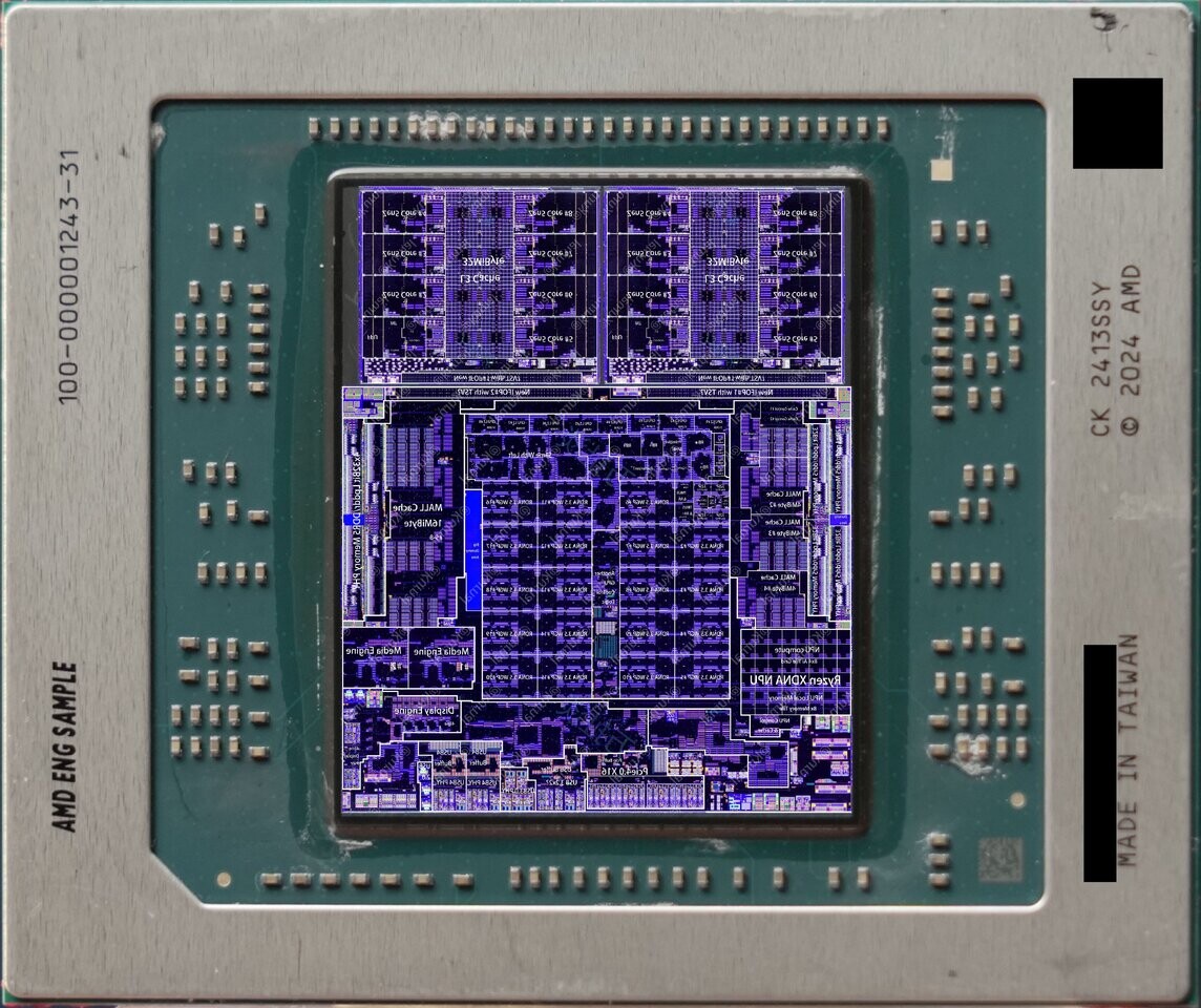
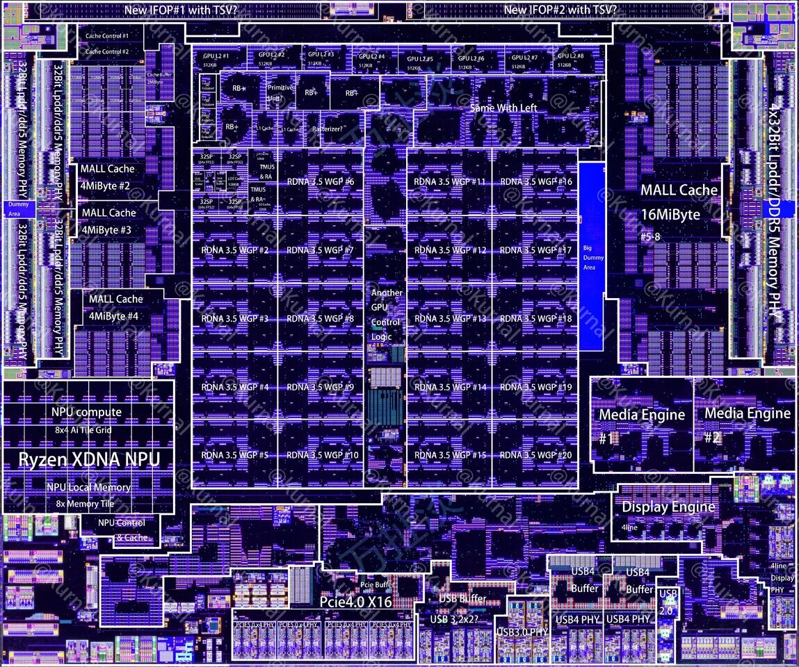
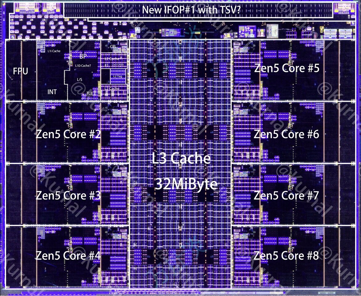
AMD's "Strix Halo" APU, marketed as Ryzen AI Max+, has just been exposed in die-shot analysis. Confirming the processor's triple-die architecture, the package showcases a total silicon footprint of 441.72 mm² that integrates advanced CPU, GPU, and AI acceleration capabilities within a single package. The processor's architecture centers on two 67.07 mm² CPU CCDs, each housing eight Zen 5 cores with a dedicated 8 MB L2 cache. A substantial 307.58 mm² I/O complements these die that houses an RDNA 3.5-based integrated GPU featuring 40 CUs and AMD's XDNA 2 NPU. The memory subsystem demonstrates a 256-bit LPDDR5X interface capable of delivering 256 GB/s bandwidth, supported by 32 MB of strategically placed Last Level Cache to optimize data throughput.

The die shots reveal notable optimizations for mobile deployment, including shortened die-to-die interfaces that reduce the interconnect distance by 2 mm compared to desktop implementations. Some through-silicon via structures are present, which suggest potential compatibility with AMD's 3D V-Cache technology, though the company has not officially confirmed plans for such implementations. The I/O die integrates comprehensive connectivity options, including PCIe 4.0 x16 lanes and USB4 support, while also housing dedicated media engines with full AV1 codec support. Initial deployments of the Strix Halo APU will commence with the ASUS ROG Flow Z13 launch on February 25, marking the beginning of what AMD anticipates will be broad adoption across premium mobile computing platforms.
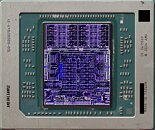
Sources: Tony Yu on Bilibili, Kurnal on X, via Tom's Hardware
Add your own comment

11 Comments on AMD Ryzen AI Max+ "Strix Halo" Die Exposed and Annotated

#1
Daven
It looks like a single CCD has an MTr/mm^2 of 128.2. That's the same as the 5090. 4 nm confirmed!
Posted on Reply
#2
Squared
AMD told Chips and Cheese that these are literally the same CCDs that go into Ryzen 9000, which is indeed using TSMC N4P.
Posted on Reply
#3
Bruno Vieira
DavenIt looks like a single CCD has an MTr/mm^2 of 128.2. That's the same as the 5090. 4 nm confirmed!
The process is called 4n, and the N stands for Nvidia. That's just the original 5nm with some Nvidia mods, just like Ada was. Its Nvidia 5nm confirmed.
SquaredAMD told Chips and Cheese that these are literally the same CCDs that go into Ryzen 9000, which is indeed using TSMC N4P.
In the same interview, they say this chip uses an organic substrate to connect the CCDs with lower latency and power than the desktop parts.
Posted on Reply
#4
AlB80
The IO looks like a regular GPU. Even USB controllers look fine. Modern graphics cards are equipped with USB-C ports.
Posted on Reply
#5
Wirko
Bruno VieiraIn the same interview, they say this chip uses an organic substrate to connect the CCDs with lower latency and power than the desktop parts.
Desktop parts use organic substrate, and the huge number of wires is the reason IOD can't be placed closer to CCDs. This APU seems to include something more advanced that enables the chips to sit next to each other. It could be Local Si Interconnect (LSI), which is approximately the TSMC's version of EMIB.
Posted on Reply
#6
Denver
AMD absolutely nailed the first generation with minimal setbacks. I never expected an MCM APU with 16 fucking cores to deliver such solid battery life while going toe-to-toe with Apple; despite using an inferior process node and lacking mac OS-level optimization. I can’t help but wonder how powerful the "Halo next-gen" will be, especially given the overwhelmingly positive reception.
Posted on Reply
#7
Tek-Check
Bruno Vieiran the same interview, they say this chip uses an organic substrate to connect the CCDs with lower latency and power than the desktop parts.
Yes, a new version of Fanout Infinity Link with organic interposer. They used something similar on Navi 31 to connect MCDs to GCD. Infinity Link brings a lot more density and bandwidth than Infinity Fabric.


It looks like they are trialing this interconnect on Strix Halo and they will implement it across Zen6 chiplets and IOD as a new high-bandwidth, low latency and high-efficiency interconnect standard. Quite exciting, indeed.

AlB80The IO looks like a regular GPU. Even USB controllers look fine. Modern graphics cards are equipped with USB-C ports.
No. Regular GPU die has less diverse logic and functions than IOD.
Some modern GPUs have USB-C port as an interface for DP video signal, and not for carrying USB or PCIe data.

On Strix Halo IOD, USB3 and USB4 PHY are additional pieces of logic, as well as NPU, which are not present on GPU die.
Posted on Reply
#8
Sound_Card
Imagine they got rid of the NPU and give up 8 more CU's.
Posted on Reply
#9
Wirko
Tek-CheckYes, a new version of Fanout Infinity Link with organic interposer. They used something similar on Navi 31 to connect MCDs to GCD. Infinity Link brings a lot more density and bandwidth than Infinity Fabric.
Is this thread same as RDL (Re-Distribution Layer)? In my (limited) understanding, RDL is a thin and dense multilayer PCB, which is bonded as a whole, or maybe built layer by layer, on top of the organic substrate, under the chiplets. AMD didn't want to disclose if they used it in Navi 31 or MI300, at least not initially.
DenverAMD absolutely nailed the first generation with minimal setbacks.
It is 1st gen but a lot of experience building MCMs has been funneled into this product. AMD could call it "Instinct AI 101", it would seem right.
Sound_CardImagine they got rid of the NPU and give up 8 more CU's.
Just an idea: CPU thread scheduling is so hard that no one can get it right these days, and "AI" has the potential to help here. If AMD and MS wanted of course.
Posted on Reply
#10
Tek-Check
Sound_CardImagine they got rid of the NPU and give up 8 more CU's.
Not now. NPU is needed for AI workloads, power management, other productivity tasks, etc. Its size takes space of 12 CUs. They need NPU on a chip like this for further development, as the next gen of NPU should go over 100 TOPS. As the logic shrinks in the next gen, they will be able to add more CUs and IO on a die.

It took them four iterations to come to this maximum size design for the package used. It's better to have such product in the market than wait another year or so for yet another lab chip iteration to be perfected. It's more practical the way it is.
WirkoIs this thread same as RDL (Re-Distribution Layer)? In my (limited) understanding, RDL is a thin and dense multilayer PCB, which is bonded as a whole, or maybe built layer by layer, on top of the organic substrate, under the chiplets. AMD didn't want to disclose if they used it in Navi 31 or MI300, at least not initially.
Final MI300 is CoWoS-S, though they did have CoWoS-R as test chip. Navi 31 uses InFO-R/oS packaging with 4 RDL layers.
semianalysis.com/2023/06/12/amd-mi300-taming-the-hype-ai-performance/

For Strix Halo, we don't know, until we know. It's either InFO-R or InFO-L, or another interation.
Posted on Reply
#11
ymdhis
I want this for desktop so much.
Posted on Reply
Add your own comment
Feb 19th, 2025 17:29 HKT change timezone

New Forum Posts

Popular Reviews

Controversial News Posts